

Every printed circuit board (PCB) consists of several layers working together to conduct electricity with specific properties, accommodate electronic components, and provide a durable and functional structure.

The base material (substrate) provides insulation and mechanical support. The most commonly used material is FR4, an epoxy laminate reinforced with fiberglass, ensuring high mechanical strength and electrical insulation. For advanced applications, such as RF devices, materials like Rogers are used for superior dielectric properties and minimal signal loss. Metal substrates like aluminum or copper are employed in heat-intensive applications such as LED systems and power electronics.

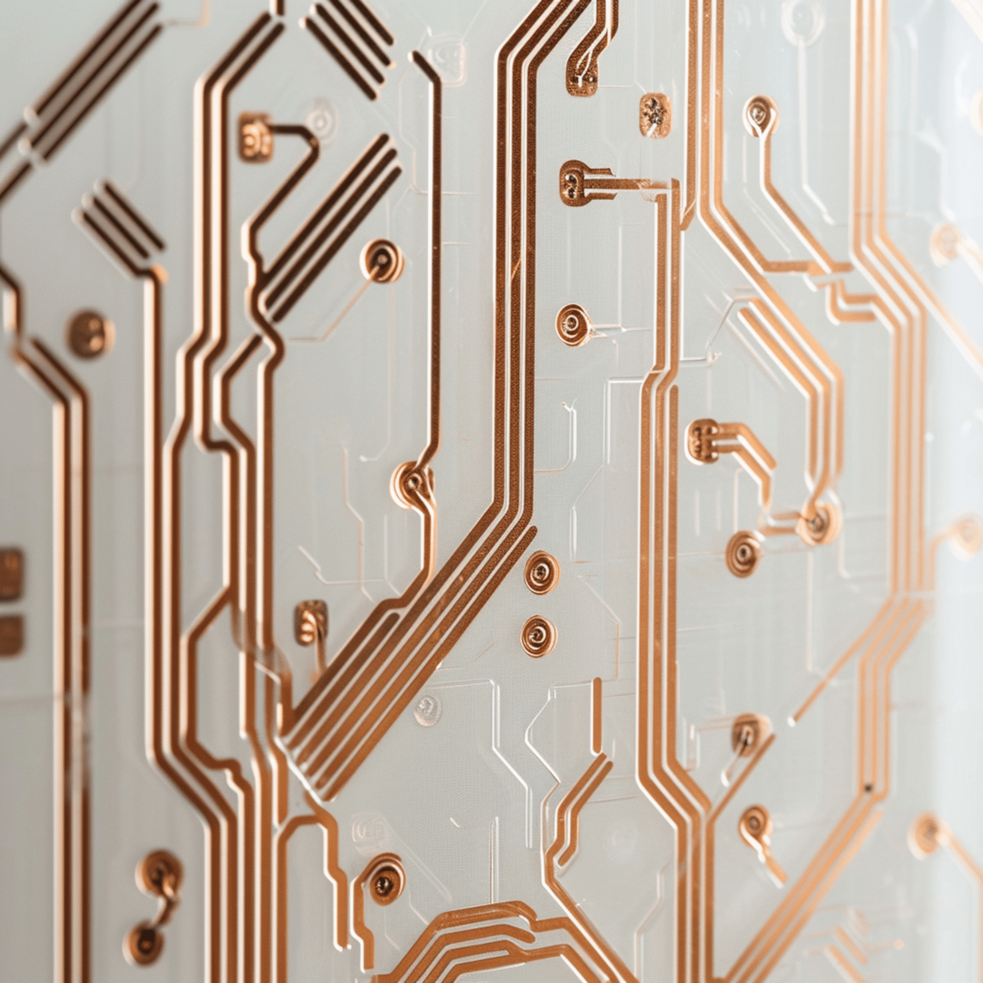
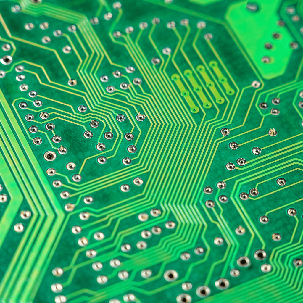
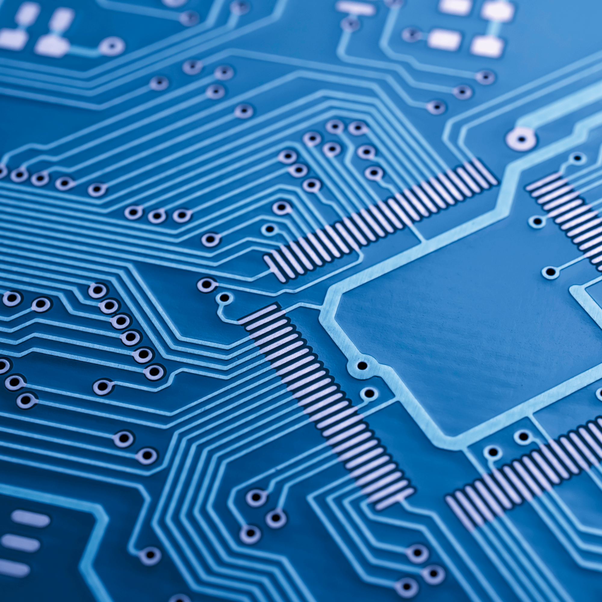
The copper layer conducts electricity between components. It is typically etched to form conductive paths. For simple designs, a single copper layer suffices, while complex designs may require multiple layers. Copper thickness can vary to meet specific requirements, improving conductivity and heat dissipation.

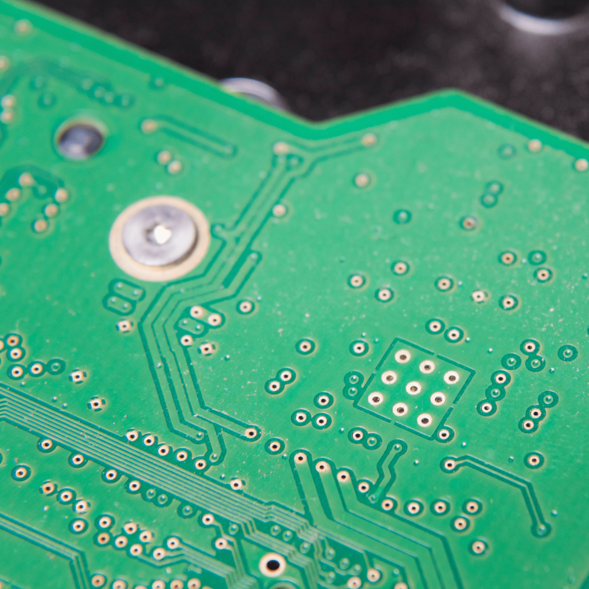
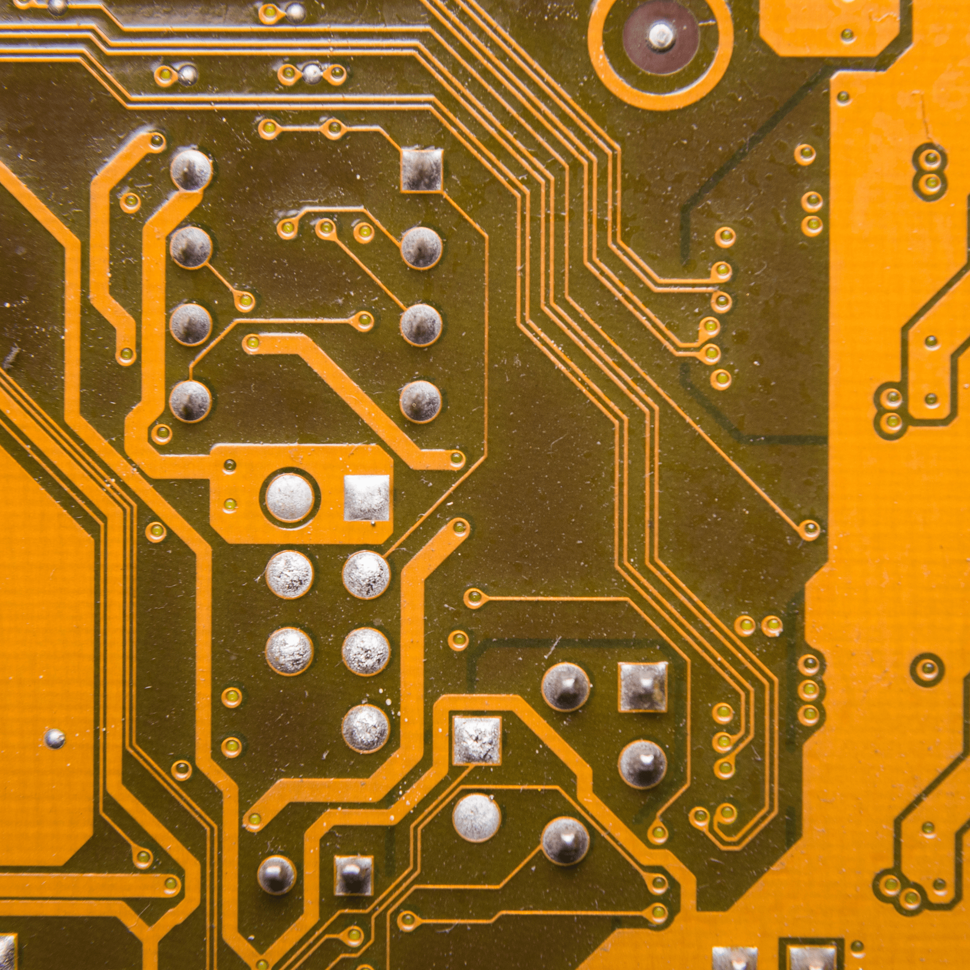
A solder mask is a protective layer applied to the copper layer to protect it from corrosion, oxidation and accidental short circuits when soldering components. The standard mask color is green, but other colors are available, such as black, white, blue or red, which can serve additional functions – for example, black masks can hinder reverse engineering and repairs. Solder masks also improve board durability and aesthetic appearance, and help with precision soldering.

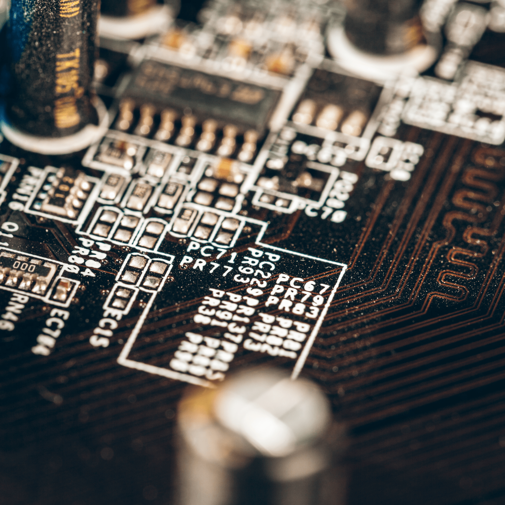
The silkscreen is a printed layer used for labeling components, paths, and other helpful markings, typically in white. It simplifies assembly, testing, and repair by providing clear visual guides.

Surface finish protects solder pads and improve their electrical properties. Options include HASL, ENIG (Electroless Nickel Immersion Gold), silver immersion, OSP (Organic Solderability Preservative), hard gold, and graphite coatings. The choice depends on application requirements, such as durability and cost.

These components work together to create a robust, functional and rugged PCB. Each of these components plays a key role in ensuring optimum mechanical, electrical and thermal properties of PCBs, and influences the cost, durability and ease of manufacturing and end-use.
The right coating protects the copper, which forms the conductive layer of the PCB, from corrosion, environmental influences, as well as improves electrical conductivity where necessary – for example, at component soldering or connector contact points. The choice of the type of PCB coating is important for its functionality and durability – it depends on the specific requirements of the application, such as temperature resistance, electrical conductivity and durability in harsh environments.
When you choose our PCBs, you can use the following types of coverings:
Choosing the right PCB surface finish depends on several key factors, such as the operating environment, service life, soldering properties and specific design requirements. Each surface finish type exhibits different advantages that affect the performance, cost and durability of the PCB. Here are some popular surface finishes and examples of proper applications:
When choosing a surface finish for your project, it is good to consider several factors, such as manufacturing cost, soldering requirements, corrosion resistance and service life in the intended operating environment. For advanced projects such as medical, telecommunications or automotive equipment, it is often recommended to choose more durable surface finish types such as ENIG or Hard Gold. If in doubt, contact our team, who can help you select the ideal surface finish for your PCB.
PCB base materials are the foundation on which all layers of a printed circuit board rest. Choosing the right base material is critical, as it affects the mechanical strength, electrical properties and thermal resistance of the board. For high-power applications or in harsh environments, choosing a base material with the right properties is essential to ensure device reliability, durability and performance. Each base material has its own specific properties that determine its use in different types of printed circuit boards, from simple consumer applications to advanced industrial electronics.
We can combine base materials to create hybrid PCBs that take advantage of the best properties of different materials. For example, combining FR-4 and Rogers optimizes cost and improves dielectric properties at high frequencies. Hybrid PCBs offer higher mechanical stability, better impedance control and lower signal loss, making them ideal for advanced applications such as telecommunications, RF and microwave radio systems.
Choosing the right PCB base material is crucial to ensure optimal performance, durability and compliance with design specifications. Different materials offer different electrical, mechanical and thermal properties, so they should be chosen based on the operating environment, type of device and specific design requirements. Below are the popular base materials and their applications:
Deciding on a specific material depends on many factors, including thermal, electrical and mechanical requirements, as well as the budget of the project. Materials such as FR-4 are common for most applications, but for more demanding designs, such as RF circuits, consider Rogers laminates, which offer better performance at high frequencies. Conversely, projects with high heat dissipation requirements, such as LED systems or power supplies, will benefit from using metal core PCBs containing aluminum or copper. If you’re not sure which material is the best fit for your project, our team can help you choose the optimal solution tailored to your specifications.
A solder mask is a thin, protective coating applied to the surface of a PCB that protects the copper traces from corrosion, dirt and accidental shorting during soldering. It makes for the most characteristic aspect of PCBs – their color.
PROPCB offers a wide range of solder mask colors:
GREEN
BLACK
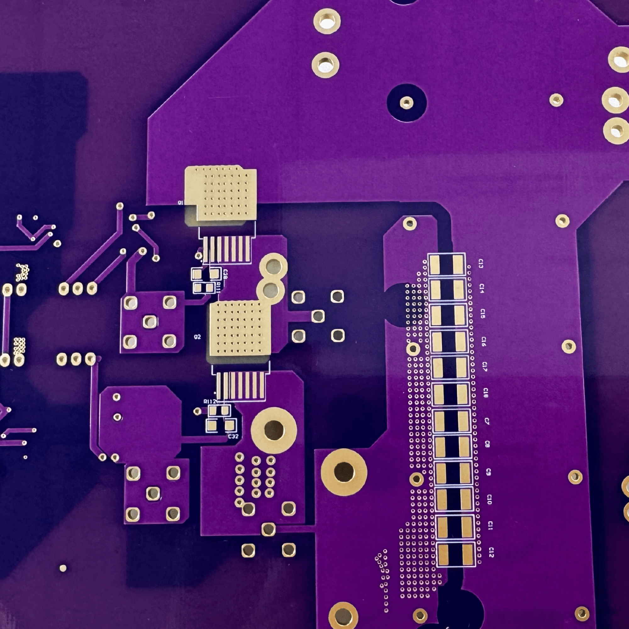
PURPLE

WHITE
YELLOW
BLUE
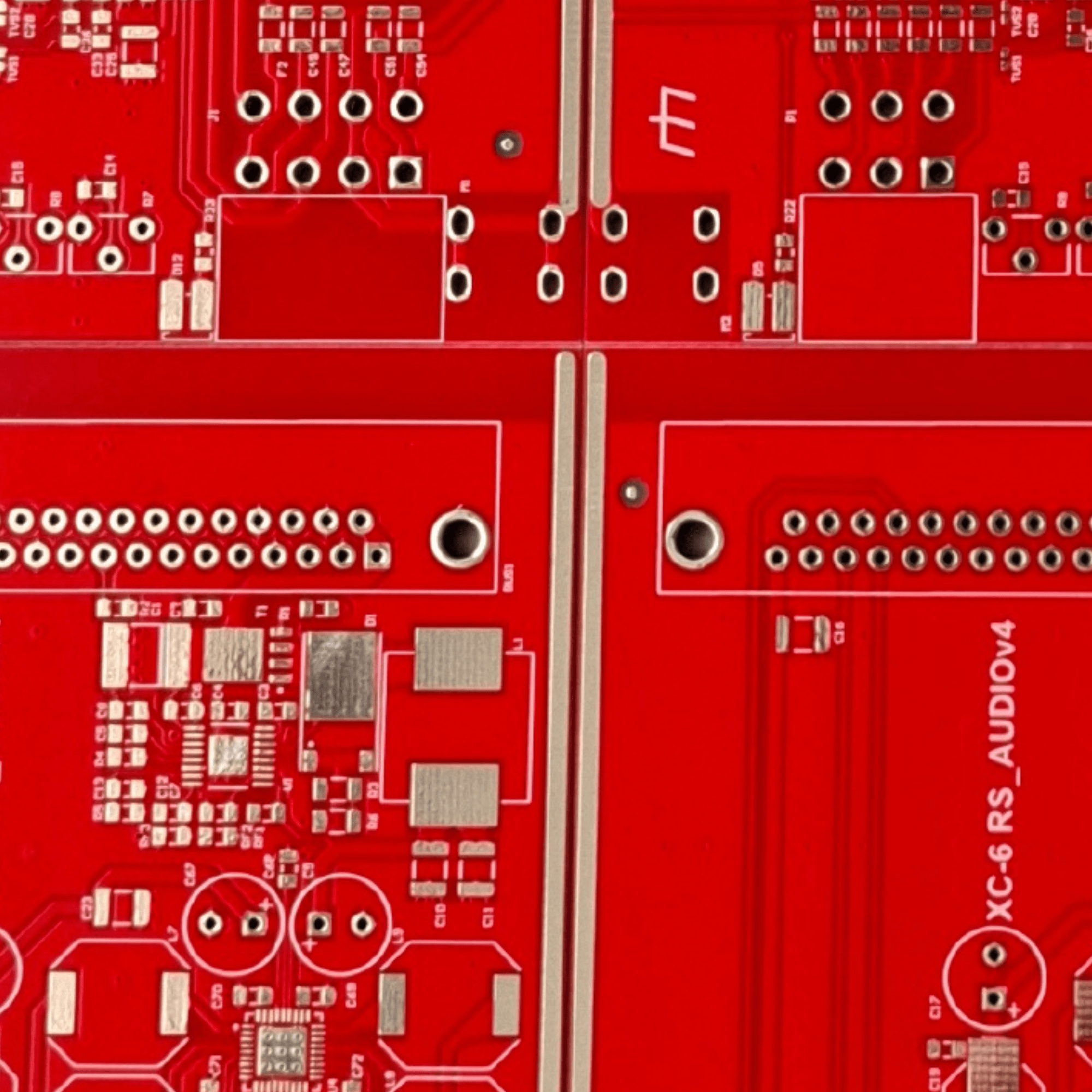
RED
The color of the solder mask is primarily aesthetic, but can also affect other aspects, such as defect identification, heat absorption and use in specific environmental conditions.
Green solder mask is the industry standard, used for its superior optical properties – highly visible contrasts and ease of defect identification. It is also most often recognized by consumers. White solder masks are often used in LED lighting because they reflect light best. Black solder masks, on the other hand, are often used to hinder reverse engineering and repairs, as they limit the visibility of paths on the board.
The choice of a specific solder mask color can affect the performance of a PCB. For example, colors such as yellow, red or blue are sometimes used for identification purposes – different production lines may use different colors to distinguish product versions. A purple solder mask, although less common, can be used for special projects or for visual distinction. In addition, dark colors, such as black soldermasks, can increase heat absorption.
In addition to color, solder masks also differ in their technical properties. For example, darker solder masks, such as black and red, can mask minor imperfections better, but are harder to see path details on, making repairs more difficult. White and light solder masks, on the other hand, are more prone to staining, but ideal for intense lighting applications.
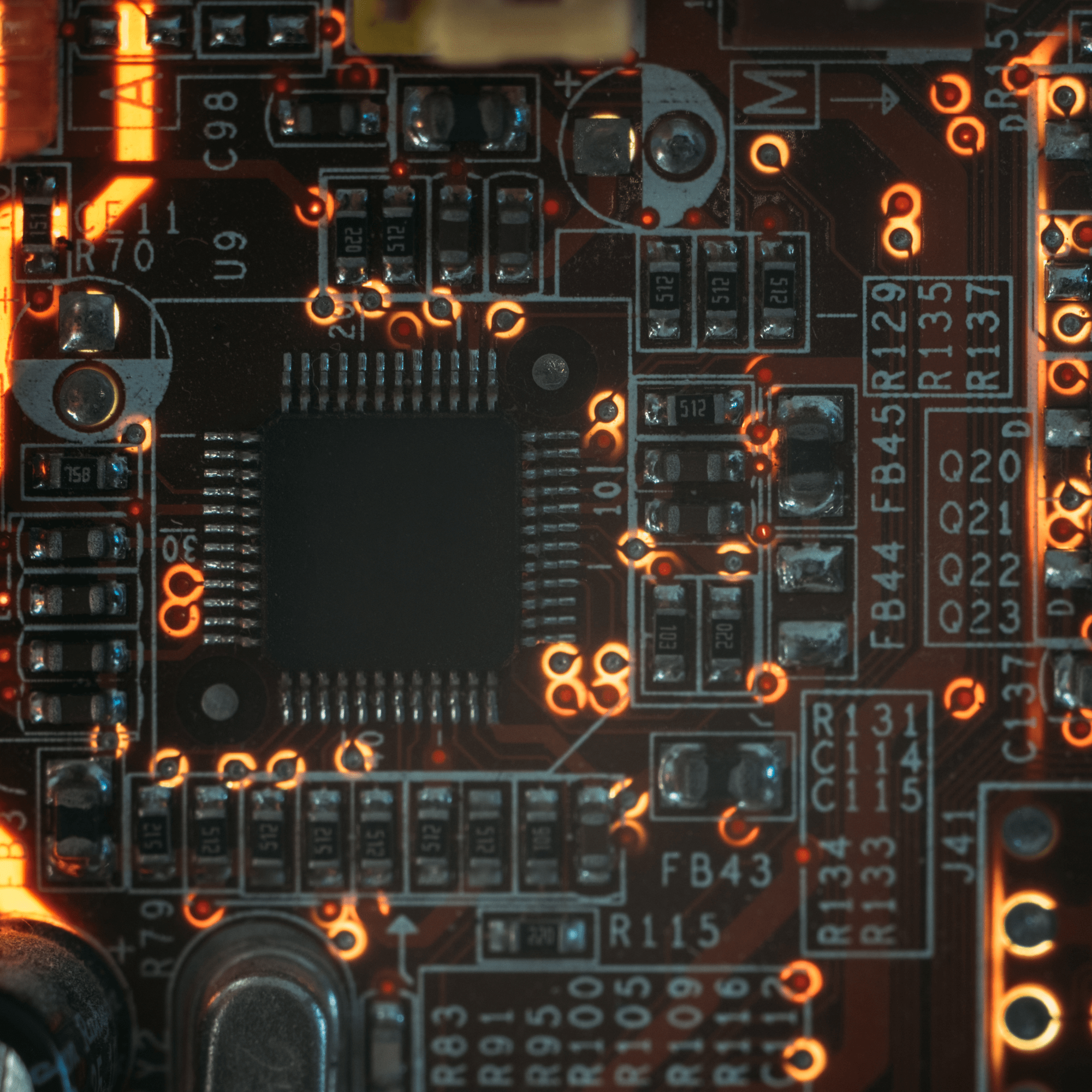
We create PCBs that suit even the most demanding requirements – from single-sided, to double-sided, to multi-layer boards up to a maximum of 40 layers. The number of layers in a PCB plays a key role depending on the complexity of the circuit. Single-sided PCBs are used in simple devices, where all traces and components are placed on one side. Double-sided PCBs allow paths to be routed on both sides for increased functionality. Multilayer PCBs allow for more complex designs with more connections, better signal integrity and reduced electromagnetic interference (EMI). Interconnections between layers are realized with vias, which allow signals to pass between different levels. Our technological processes allow the production of PCBs with up to 40 layers and high interconnection density, enabling high performance and projects in modern applications – such as servers, medical devices, telecommunications and automotive industries.
The choice of the number of layers for a PCB design depends on a number of factors, such as the complexity of the design, the number of connections between components, and signal and noise management requirements. Single-layer PCBs are sufficient for simple devices with a small number of components, such as remote controls or sensors. Double-sided PCBs are used where more tracks and more complex connections are required. Multilayer PCBs, consisting of three or more layers, are ideal for designs where signal integrity and EMI reduction are critical, as in telecommunications equipment, servers or advanced medical electronics. Projects requiring high-density connectivity and high power use up to 40 layers, allowing maximum performance in limited space. When choosing the number of layers, it is also important to take into account other factors, such as the manufacturing cost – the more layers, the more complex and expensive the manufacturing process is. Optimizing the number of layers allows for efficient management of space, cost and circuit performance.
Vias are critical components in multilayer PCBs, enabling connections between traces across different layers of the board. There are several types of vias that aid in managing connections and space within a PCB:
 w PCB wielowarstwowych-min")
The appropriate selection of vias is essential for signal integrity and space optimization in multilayer PCBs. These technologies significantly increase the number of connections in space-constrained projects, while ensuring high performance and reliability of circuits.
Single-layer PCBs are the best choice for simple applications where the number of components and traces is limited. They are ideal for manufacturing low-cost devices such as calculators, watches, remote controls, toys, and sensors. Due to their straightforward construction, single-layer PCBs are quick and inexpensive to produce, making them a perfect solution for mass-market devices where complex electrical connections are unnecessary. This type of board also excels in applications where size and circuit complexity are not critical factors.
Trace density and PCB dimensions are critical factors in designing advanced circuits. High trace density enables more complex designs within limited space, which is particularly important in modern electronic devices that must be compact yet highly functional.
HDI (High Density Interconnect) boards feature minimal trace widths and via sizes, allowing for the placement of more components within a smaller area. This technology enables the creation of intricate connections in devices such as smartphones, tablets, medical equipment, and military devices. The use of microvias and blind vias in HDI PCBs facilitates better circuit integration, reduces signal delays, and improves electrical performance in complex multilayer projects.
The thickness of the copper layer significantly impacts a PCB’s thermal performance and electrical efficiency. Thicker copper layers enhance the board’s ability to dissipate heat, which is essential for high-power applications such as LED systems, power converters, and industrial electronics.
Thicker copper layers also increase the durability of traces under high current loads, improving the longevity and performance of the PCB in demanding environments such as automotive and heavy industry.
Thanks to advanced manufacturing technologies, at PROPCB we are able to realize high-precision circuits with high path density, with a minimum path width of 3 mils (0.076 mm) and a spacing between paths of 3 mils as well. We also offer holes with a minimum diameter of 6 mils (0.15 mm) for mechanical drilling and 4 mils (0.1 mm) for laser holes, allowing for even greater miniaturization and better space management in complex multilayer designs.
PROPCB delivers PCBs with maximum dimensions of up to 800 x 1500 mm, allowing for large projects that require a larger assembly area. In addition to standard dimensions, our technologies also allow for customization of trace thickness from 0.2 mm up to 10 mm, giving customers a wide range of design options, both in space-constrained applications and in projects requiring greater mechanical strength.
Our advanced manufacturing capabilities enable us to create printed circuit boards with complex interconnections that meet demanding technical requirements, ideally suited for projects in industries such as automotive, consumer electronics, telecommunication and industrial applications.


