

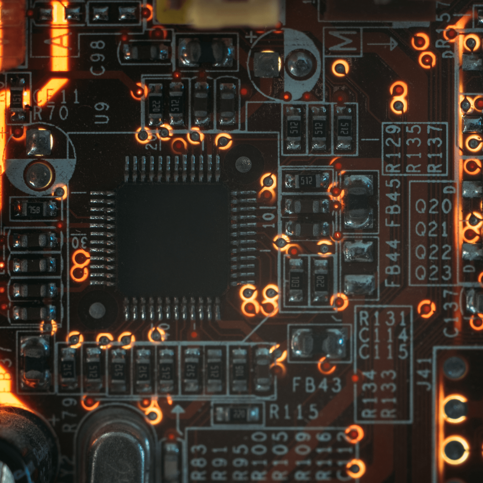
Our offer includes a wide range of PCB production technologies, from single- and double-sided boards to multilayer boards, with the capability to produce up to 40 layers. We provide precise execution and reliability for both prototyping and mass production projects.
The choice of base material is crucial for the durability, performance, and reliability of PCBs. When selecting PROPCB for your project, you have access to a range of substrate solutions:

Surface finishes help protect the solderable areas from corrosion and improve their conductivity. PROPCB offers a wide range of surface finishes for your projects:
Choosing the solder mask color matters. Our variety of PCB solder mask colors allows customization of both the aesthetics and functionality of your board to meet the specific needs of your project. Colors such as green, white, black, or blue can aid in identifying and segregating different product versions or circuits in complex systems. Additionally, color can impact trace visibility during inspection – green offers the best detail visibility, white aids in heat absorption, making it ideal for LED applications, while black hampers reverse engineering, ensuring greater intellectual security.
AVAILABLE SOLDER MASK COLORS:
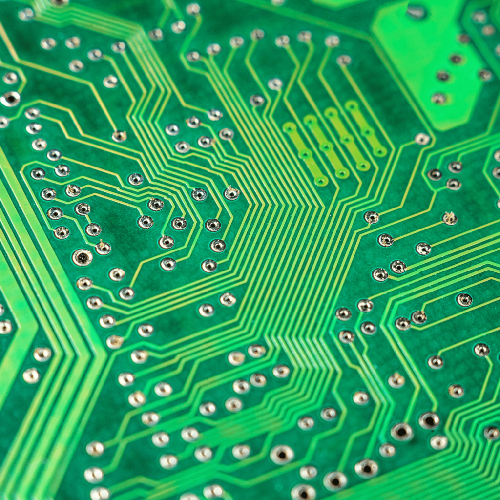
GREEN
BLACK
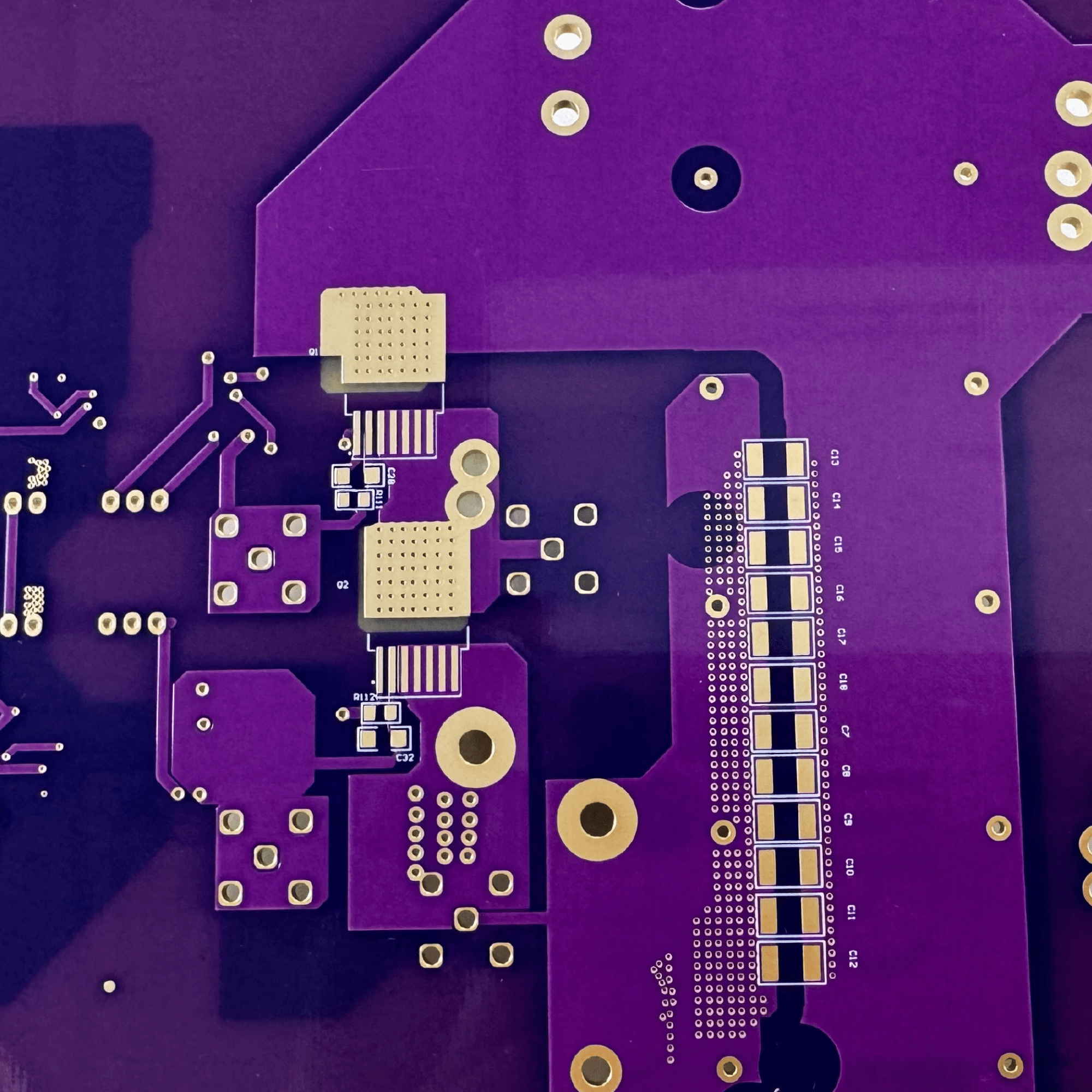
PURPLE

WHITE
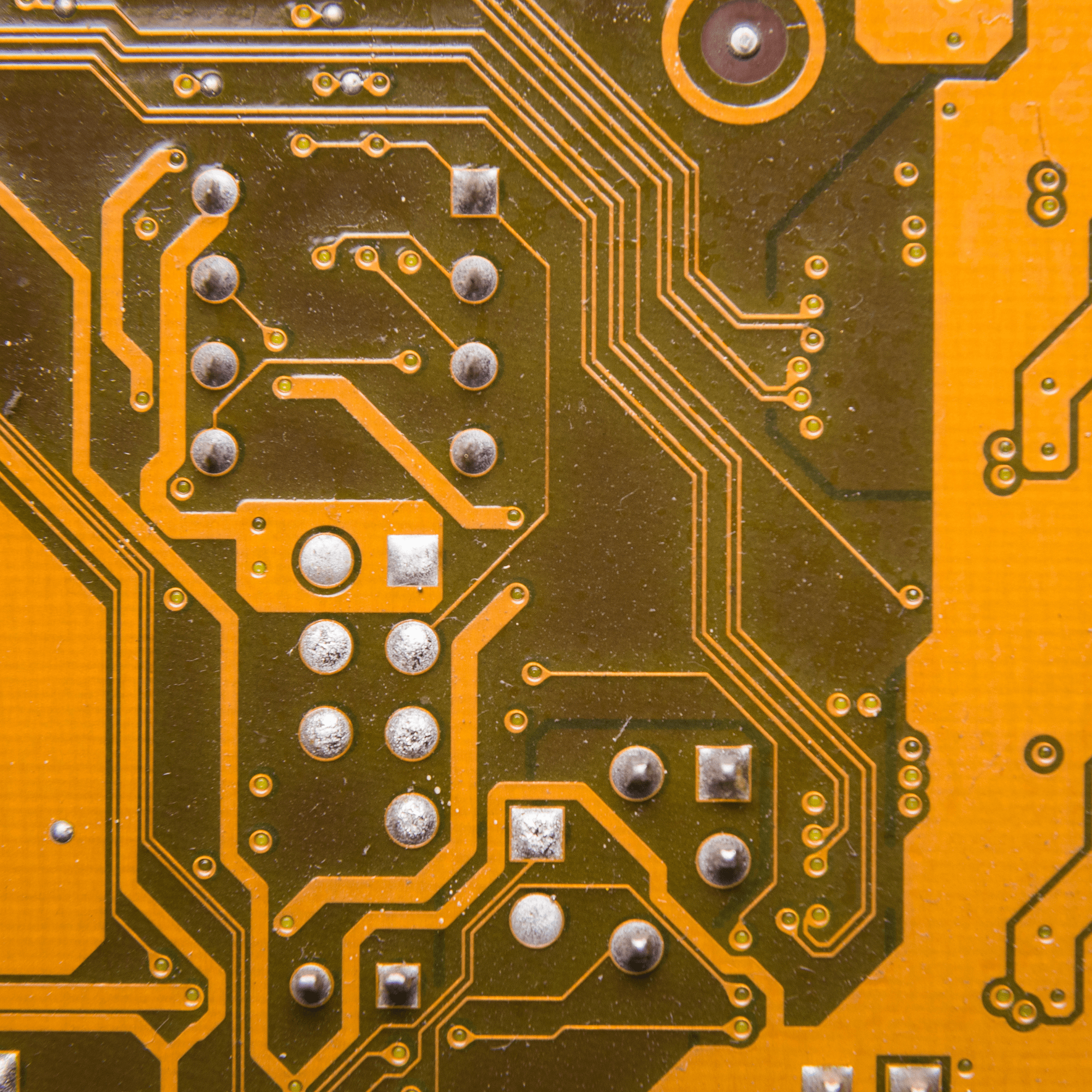
YELLOW
BLUE
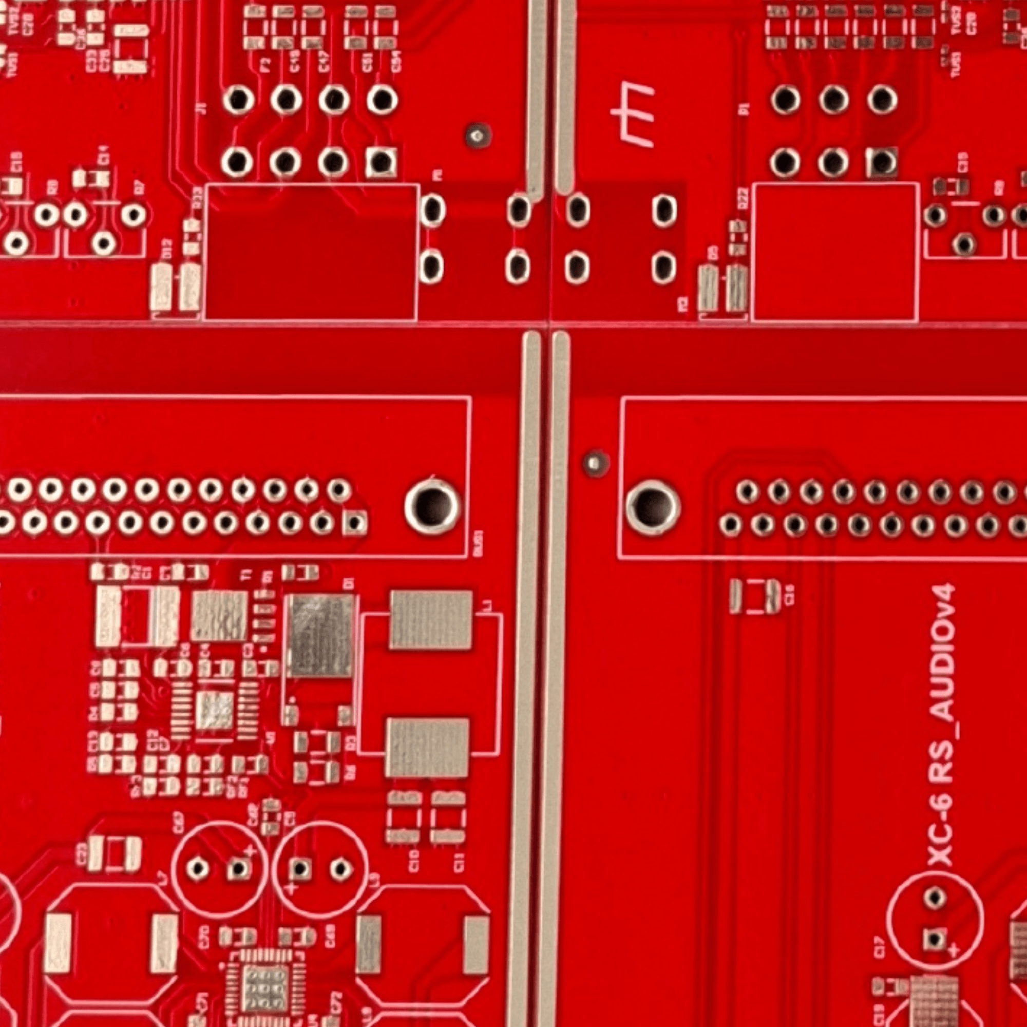
RED
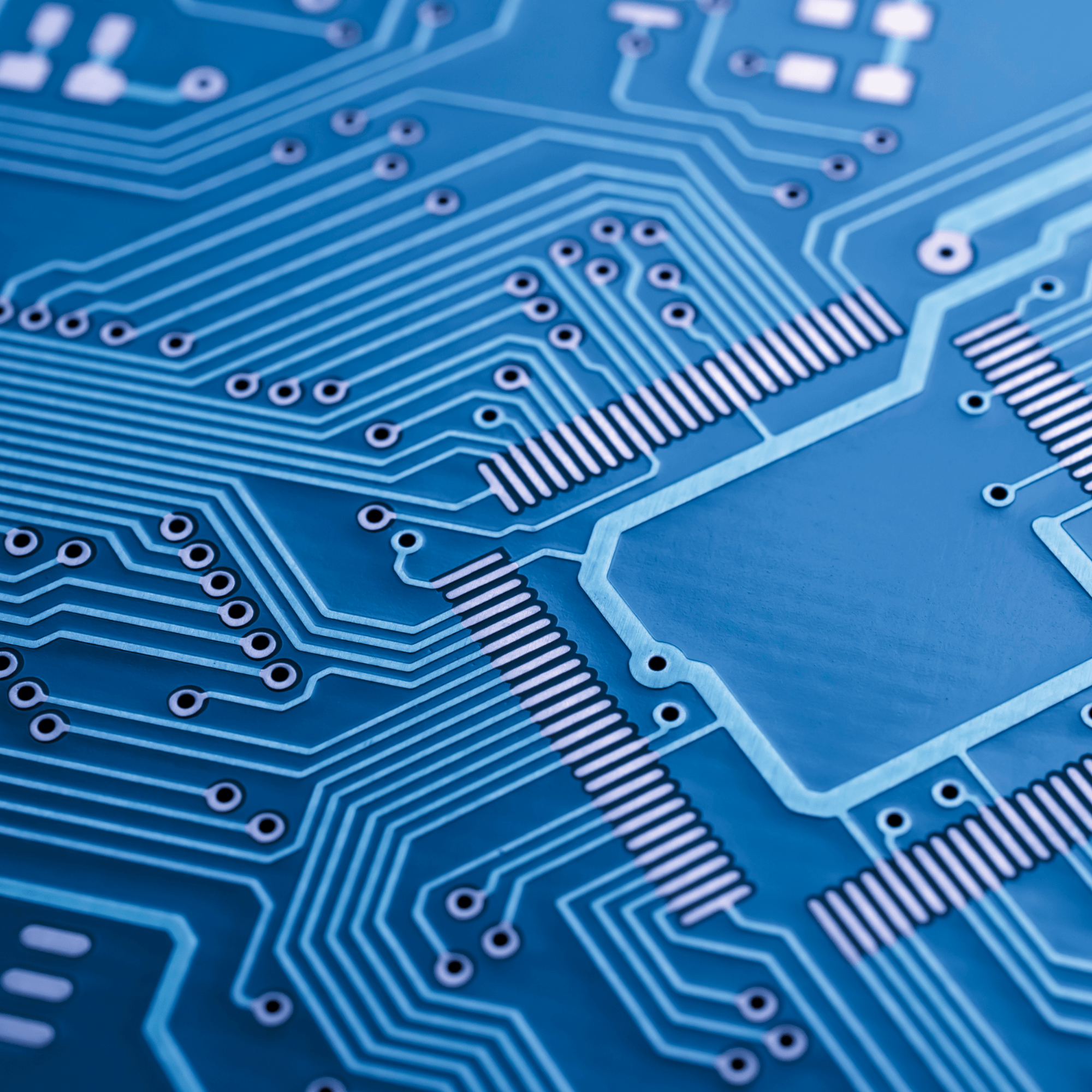
Our PCBs are characterized by high precision and trace density. We offer maximum copper thickness of up to 12 oz (420 μm) and minimum trace width and spacing of 3 mil, making them suitable for advanced high-power and high-frequency projects.
Want to know more details? Download the full specification table of our technology and choose the solutions best suited to your project!

Do you have a vision you want to bring to life? Our team of experts is ready to assist you at every stage – from design to production. Fill out the form, and we’ll get back to you quickly to discuss details and create something extraordinary together. We’re waiting for your message!
