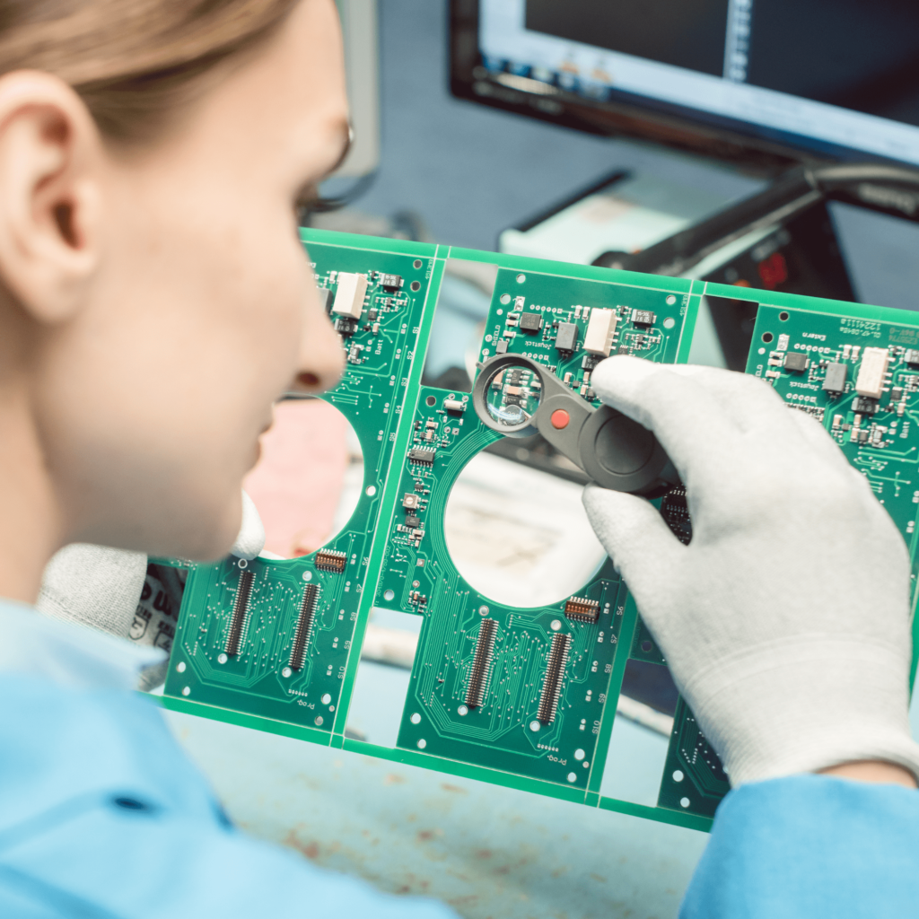
PCB PRODUCTION PROCESS

At PROPCB, we have meticulously developed our PCB production process to ensure maximum efficiency, precision, and customization to meet our clients’ specific needs. Every stage – from quotation to delivery – has been optimized to guarantee the highest quality and on-time completion. Our advanced technologies allow us to produce various types of PCBs, meeting every design challenge.

QUOTATION AND TECHNICAL CONSULTATIONS

The first step involves discussing technologies and materials with the client to tailor the choice of base material, number of layers, and surface finish to the technical and budgetary requirements of the project. Our experts support the client in selecting suitable technological solutions, such as:

  • Base Material: FR4, Rogers, IMS (aluminum or copper) depending on project requirements like heat management or signal stability.
  • Number of Layers: From single-sided to multilayer, up to 40 layers.
  • Surface Finishes: HASL, ENIG, OSP, or others, depending on solderability, durability, and conductivity needs.

During this stage, we also discuss advanced requirements, such as impedance control, RF circuit specifications, or HDI needs, which are critical for complex projects like medical, telecommunications, or automotive devices.

After agreeing on technical details, we proceed to a detailed cost calculation. Our pricing systems provide fast, accurate, and competitive quotes, factoring in all project specifications, order size, and lead times. With advanced tools and experience, we can quickly present competitive offers for both small prototype batches and large-scale production.

Upon quotation approval, we conduct a thorough design file verification. Our engineers review the project files for potential errors that may affect PCB quality or functionality. This review includes:

  • Connection Accuracy Analysis
  • Dimension and Technical Specification Verification
  • Compatibility Check with Production Technologies, such as impedance control for RF or microwave circuits.

Only after these three stages are complete are the design files approved for physical production. This meticulous initial control minimizes production errors and ensures the final PCBs fully meet the client’s requirements.

PCB PRODUCTION IN THE FACTORY – STEP-BY-STEP

PCB production is a complex process involving multiple stages that require advanced technology and precision. Each board undergoes a series of sophisticated operations to ensure the highest quality and reliability of the finished printed circuits.

Once the technical specifications and pricing are approved, the first step is to prepare the design mask. PCB design files are converted into masks that map the copper connections on the PCB layers. Each copper layer, as well as the descriptive layers and solder masks, are accurately mapped based on the supplied design. Depending on the number of PCB layers (single-sided, double-sided, multilayer), appropriate masks are prepared. For multilayer PCBs, additional power and ground layers are designed to ensure signal integrity and reduce interference.

In this step, holes are drilled in the PCB and vias are placed. Vias connect the different layers of the PCB – both the outer layers and the inner layers in the case of multilayer boards. The holes can be made mechanically or by laser, depending on the requirements of the project. There are several types of vias – through vias pass through all layers of the board, while blind vias and buried vias connect select layers, which optimizes space on the board. Microvias are used in HDI printed circuits, in order to obtain higher connection density. Laser tools are used to make the holes to achieve the highest degree of precision – after all, vias are highly structurally important components of PCBs.

A thin layer of copper is applied to the substrate (usually FR4). For multilayer PCBs, lamination is done repeatedly, combining layers of copper and insulating material. Each layer is later etched in order to isolate the conductive paths. This process requires great precision, especially in high-density interconnection (HDI) boards, where the paths must be very thin. In subsequent steps, additional layers of copper and insulation are applied to create more connections between components. For more advanced designs, such as RF circuits, special low dielectricity materials are used to minimize signal loss.

In subsequent steps, additional layers of copper and insulation are applied to create more connections between components. For more advanced designs, such as RF circuits, special low dielectricity materials are used to minimize signal loss.

After adding copper layers, their surface is etched to create conductive paths that conform to the design. A photoresistive material is used to protect the copper from etching where it is to remain. This process ensures that the copper paths are accurately mapped and form optimal electrical connections. In multilayer PCBs, each copper layer must be etched separately, and then bonded to the other layers including vias. In the case of HDI PCBs, micro vias and blind vias are used to provide better connection placement.

After applying layers of copper and mask, surface finishes are applied. This coating provides long-term protection of solder points from corrosion and improves their conductivity. Depending on customer specifications, different surface finish coating types are used, such as:
HASL (Hot Air Solder Leveling): A solder coating that offers good solderability and protection against oxidation.

ENIG (Electroless Nickel Immersion Gold): Nickel-gold plating, ideal for projects requiring high reliability and durability.OSP (Organic Solderability Preservative): An economical solution to protect copper from oxidation.

A descriptive layer, or silkscreen, is applied over the applied solder mask to mark components, tracks and other information on the PCB. These markings make it easier to assemble, test and repair the board, ensuring legibility for those operating the equipment.

After applying layers of copper and mask, surface coating provides long-term protection of solder points from corrosion and improves their conductivity. Depending on customer specifications, different coating techniques are used, such as:

  • HASL (Hot Air Solder Leveling): A solder coating that offers good solderability and protection against oxidation.
  • ENIG (Electroless Nickel Immersion Gold): Nickel-gold plating, ideal for projects requiring high reliability and durability.
  • OSP (Organic Solderability Preservative): An economical solution to protect copper from oxidation.

Production panels contain multiple PCBs – so they need to be separated and prepared in a way that is appropriate to the customer’s guidelines. Placing multiple PCB designs on a single panel makes it possible to speed up the production process and optimize PCB manufacturing costs.

Using a milling machine, specific PCB outlines are milled on a panel according to the design file. This allows individual PCBs to be separated, leaving a smooth edge surface. PCBs can also be profiled with a V-groove (also called V-cut and V-scoring) using a special machine. This allows individual PCBs to be easily separated after assembly, which is useful for automated component assembly.

Finally, all PCBs are thoroughly cleaned to remove dust and debris remaining on the PCBs, as well as inside the holes and grooves.

Each board is subjected to rigorous quality control – as they are the foundation for components that perform specific tasks.

Using specialized machines, the PCBs are tested electrically to verify that the paths are properly connected, and to find short circuits and breaks in the circuits. The thermal conductivity of the board – important for automotive applications and those using high-power components – is also tested, as well as the impedance of the circuits, to ensure that the conductivity is as required and the board will function without interference.

PCBs undergo automatic optical inspection for manufacturing defects that may affect the performance of the finished product; there is also an inspection of PCB dimensions and edge finish. In addition, it is possible to perform functional tests, where the operation of the PCB is simulated in real time.

It is worth noting that the production process shown may vary depending on the type of substrate or PCB chosen. Regardless of the customer’s choice, we always strive to provide the best PCBs, ensuring the highest quality and full compliance with customer guidelines.

QUALITY CONTROL AND TESTING

At PROPCB, we place particular emphasis on quality control to ensure reliability and compliance with client specifications. Each PCB undergoes rigorous testing to eliminate potential errors and meet the highest quality standards.

Each printed circuit is subjected to an electrical test (E-test), which verifies the correctness of the electrical connections and the continuity of the paths. During this test, the PCB is connected to a system that analyzes whether the paths conduct electricity in the right way, eliminating the risk of short circuits or breaks. This test is particularly important in multilayer PCBs and HDI, where the number of connections is much higher.

For IMS circuits and applications requiring advanced thermal management (e.g., LED systems, high-power electronics), we perform thermal tests. The purpose of these tests is to verify that the board effectively dissipates heat, ensuring the stability and reliability of electronic components, even under harsh conditions. These tests are crucial in automotive and industrial applications where circuits must operate at extreme temperatures.

For RF, microwave and telecom PCBs, we perform impedance tests, which check signal stability and minimize interference. These tests are extremely important in applications requiring high-precision data transmission, such as radio systems, 5G devices and radar. Correct impedance ensures that electrical signals travel without loss, which is crucial to the proper operation of devices.

Each PCB also undergoes a visual inspection, which can detect physical defects such as excessive copper build-up, solder mask errors or improperly made holes. We also use automatic optical testing (AOI), which ensures that all board components are correctly positioned and in accordance with the design.

In some cases, especially in mass production for advanced applications, we conduct functional tests, which simulate the conditions of actual PCB use. This allows us to make sure that the finished product will perform as expected, even in demanding environments such as automotive, industrial, telecommunications or medical.

Our advanced quality control and extensive testing ensure that every PCB that leaves our production lines meets the highest standards of quality and reliability. Through these measures, we minimize the risk of manufacturing defects and ensure that the final product performs flawlessly.

FINALIZATION AND DELIVERY

After passing all quality checks, PCBs are finalized and prepared for shipment. Each board is carefully packaged to prevent mechanical damage, moisture, or other external factors during transport.

Secure Packaging

For each PCB we use special packaging methods, which we adapt to the type of circuits ordered. For flexible and rigid-flexible PCBs, we use special inserts that protect them from bending during transport. Multilayer and HDI PCBs, on the other hand, are packed in antistatic packaging that protects them from electrostatic charges that can damage delicate tracks and components.

Delivery options

We offer a variety of delivery options, including express shipping to deliver finished PCBs on time, regardless of the customer’s location. Our delivery times are tailored to the specifics of the order. We work closely with international logistics companies to ensure fast and safe delivery, for both domestic and international customers. Our tracking systems allow us to monitor shipments at every stage of transportation.

After-sales support

Once the product is delivered, PROPCB provides full after-sales support, helping customers resolve any questions or problems that may arise during PCB assembly or use. Our team is available to provide technical assistance and advice on further production optimization or the introduction of new technological solutions.

Finalization of production and delivery is not only the closure of the process, but also our guarantee that the finished product meets all requirements, both technically and logistically.